
Professor Ertugrul Cubukcu

Research Interests
Some of our projects:
-
‣optoelectronic nanodevices
-
‣plasmomechanics
-
‣nano-biochemical sensing
-
‣graphene photonics
-
‣2D semiconductor materials
-
‣nonlinear optical devices

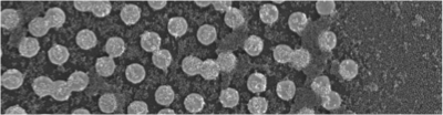
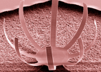
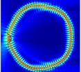
Multimodal graphene enabled biosensor: With this device we experimentally achieve an ultra-wide linear dynamic sensing range of 5 orders of magnitude of protein concentration, an improvement over state-of-the-art single mode nanosensors by approximately 2-3 orders of magnitude. This device uniquely combines different transduction schemes on the same chip. (a) Nanoelectronic mode relies on an integrated graphene field effect transistor (FET). The peak in the source-drain resistance vs gate voltage corresponds to the Fermi level. Upon biochemical adsorption the effective doping will change the Fermi level, which is used as the electronic transduction method. (b) The nanophotonic sensing mode relies on a nanoantenna based perfect absorber. The peak corresponds to the plasmonic resonance of the structure, which is sensitive to the refractive index of the local environment. Inset: SEM image of an array of nanoantennas. (c) The nanomechanical mode of the sensor is based on a high quality factor (Q~10,000) silicon nitride membrane resonator. The mechanical resonance frequency changes as a result of mass changes upon protein binding. See our paper


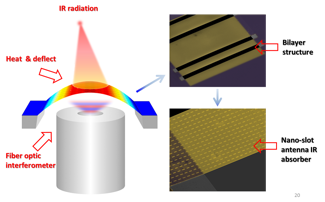
We have demonstrated a new plasmo-thermomechanical device, which integrates thermoplasmonic effects with nanomechanics using light absorption by plasmonic nanoantennas as the nanoscale heat source inducing thermomechanical actuation. As one specific example of the platform, we report a novel room temperature thermal infrared detector that integrates a nanoplasmonic absorber on a beam type nanomechanical structure. Our nanoplasmonic thermomechanical device relies on efficient absorption of infrared radiation by an array of nanoslot antennas as an active component that converts optical power into heat. The nanoslot configuration provides the best thermomechanical coupling due to its uniform bilayer material coverage as compared to an array of discrete nanoantenna elements. The generated heat is then converted to a temperature increase on the integrated nanomechanical bimaterial structure. In response to this temperature increase, the bimaterial nanomechanical beam bends as a result of the differences in the thermal expansion coefficients of the two constituent materials. An integrated fiber-based interferometric readout, which offers the best displacement sensitivity, then converts this mechanical bending into an electrical signal.
See our paper

We demonstrate an electrically tunable plasmonic absorber with near unity absorption enabled by indium tin oxide (ITO) as the active material.
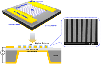
The schematic of the electrically tunable plasmonic absorber is shown in Figure. Periodic gold nanostrips are fabricated on top of a free standing silicon nitride membrane with a silicon frame using standard electron beam lithography and lift-off processes. The backside of the nitride membrane spacer is coated with a 100 nm thick gold layer, acting simultaneously as the back electrode and the back reflector allowing for near unity absorption in the plasmonic absorber design first proposed by Shvets et al. 3 The gold nanostrips and back plate also act as the top and bottom contact electrodes for carrier injection and electrostatic gating, respectively. For electrical tunability, a thin layer of ITO is then deposited directly on the nanostrip antennas, where the near field intensity is maximum.
See our paper